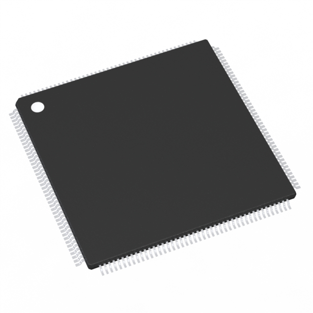
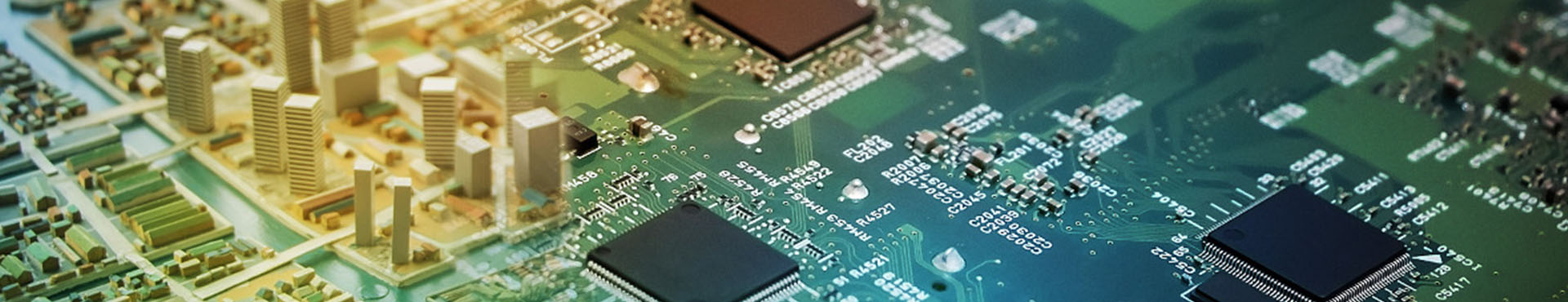
In the realm of miniaturized electronics where space is measured in microns and performance cannot be compromised, the substrate material and thickness become defining factors. The Ultra-thin BT PCB has emerged as the preferred platform for applications demanding exceptional dimensional stability, superior electrical properties, and minimal thickness. HONTEC has established itself as a trusted manufacturer of Ultra-thin BT PCB solutions, serving high-tech industries across 28 countries with specialized expertise in high-mix, low-volume, and quick-turn prototype production.
BT epoxy resin, or bismaleimide triazine, offers a unique combination of properties that make it ideal for thin-profile applications. With high glass transition temperature, low moisture absorption, and excellent dimensional stability, Ultra-thin BT PCB construction supports fine-pitch component assembly and maintains reliability under thermal cycling. Applications ranging from mobile devices and wearable electronics to semiconductor packaging and advanced sensor systems increasingly depend on Ultra-thin BT PCB technology to meet aggressive size and performance targets.
Смештен у Шенжену, Гуангдонг, ХОНТЕЦ комбинује напредне производне могућности са ригорозним стандардима квалитета. Сваки произведени ултра-танак БТ ПЦБ носи гаранцију УЛ, СГС и ИСО9001 сертификата, док компанија активно примењује стандарде ИСО14001 и ТС16949. Са логистичким партнерствима која укључују УПС, ДХЛ и шпедитере светске класе, ХОНТЕЦ обезбеђује ефикасну глобалну испоруку. Сваки упит добија одговор у року од 24 сата, што одражава посвећеност одговору коју глобални инжењерски тимови цене.
BT epoxy resin possesses a combination of material properties that make it exceptionally well-suited for Ultra-thin BT PCB fabrication. The high glass transition temperature of BT material, typically ranging from 180°C to 230°C, ensures that the substrate maintains mechanical integrity and dimensional stability even under elevated temperatures encountered during assembly and operation. This high Tg characteristic is particularly valuable for thin boards, as thinner substrates are inherently more susceptible to warpage and dimensional changes under thermal stress. The low moisture absorption of BT material, typically below 0.5%, prevents the dimensional instability and dielectric property shifts that can occur when hygroscopic materials absorb moisture. For Ultra-thin BT PCB designs, this stability translates to consistent impedance control and reliable fine-pitch component assembly. The coefficient of thermal expansion of BT closely matches that of silicon, reducing mechanical stress on solder joints when boards undergo thermal cycling—a critical consideration for thin boards that have less material to absorb thermal expansion forces. Additionally, BT material exhibits excellent dielectric properties with low dissipation factor, supporting high-frequency signal integrity even in thin constructions. HONTEC leverages these material advantages to deliver Ultra-thin BT PCB products that maintain reliability and electrical performance across demanding applications.
Fabricating Ultra-thin BT PCB products requires specialized processes that address the unique challenges of handling and processing thin, delicate substrates. HONTEC employs dedicated handling systems designed specifically for thin-board processing, including automated panel support systems that prevent flexing and stress during fabrication. The imaging process for thin BT substrates utilizes low-tension handling and precision alignment systems that maintain registration accuracy across the board surface without inducing distortion. Etching processes are optimized for the thin copper cladding typically used with BT materials, with controlled chemistry and conveyor speeds that achieve clean trace definition without over-etching. Lamination of Ultra-thin BT PCB constructions employs press cycles with carefully controlled pressure profiles that prevent resin flow irregularities while ensuring complete bonding between layers. Laser drilling, rather than mechanical drilling, is utilized for via formation in many thin BT applications, as laser processes provide the precision required for small via diameters without exerting mechanical stress that could damage thin materials. HONTEC implements additional quality checks specifically for thin boards, including warpage measurement, surface profile analysis, and enhanced optical inspection that detects defects that might be more critical in thin constructions. This specialized approach ensures that Ultra-thin BT PCB products meet the stringent quality requirements of compact electronic assemblies.
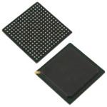
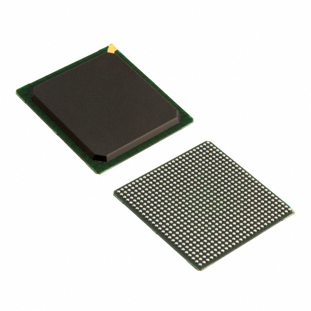
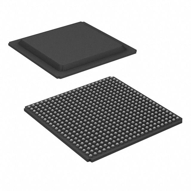
Ultra-thin BT PCB technology delivers maximum value in applications where space constraints, electrical performance, and reliability converge. Semiconductor packaging represents one of the largest application areas, with Ultra-thin BT PCB serving as substrate for chip-scale packages, system-in-package modules, and advanced memory devices. The thin profile and stable electrical properties of BT material support the fine lines and tight tolerances required for high-density interconnect in packaging applications. Mobile devices, including smartphones, tablets, and wearables, utilize Ultra-thin BT PCB construction for antenna modules, camera modules, and display interfaces where space is at a premium and signal integrity cannot be compromised. Medical devices, particularly implantable and wearable applications, benefit from the biocompatibility, thin profile, and reliability of BT substrates. HONTEC advises clients on design considerations specific to thin BT fabrication, including trace width and spacing requirements for different copper weights, via design rules for thin materials, and panelization strategies that optimize yield while maintaining board flatness. The engineering team also provides guidance on impedance control for thin constructions, where dielectric thickness variations have proportionally greater impact on characteristic impedance than in thicker boards. By addressing these considerations during design, clients achieve Ultra-thin BT PCB solutions that realize the full benefits of BT material while maintaining manufacturability and reliability.
ХОНТЕЦ одржава производне могућности које обухватају читав низ захтева за ултра-танку БТ ПЦБ. Подржане су дебљине готових плоча од 0,1 мм до 0,8 мм, са бројем слојева који одговара сложености дизајна и ограничењима дебљине. Тегови бакра од 0,25 оз до 1 оз задовољавају потребе за глодањем финог корака и струјом унутар танких профила.
Surface finish selections for Ultra-thin BT PCB applications include ENIG for flat surfaces that support fine-pitch component assembly, immersion silver for solderability requirements, and ENEPIG for applications requiring wire bonding compatibility. HONTEC supports advanced via structures including microvias and filled vias that maintain surface flatness for component placement.
За инжењерске тимове који траже производног партнера способног да испоруче поуздана Ултра-танка БТ ПЦБ решења од прототипа до производње, ХОНТЕЦ нуди техничку експертизу, брзу комуникацију и проверене системе квалитета подржане међународним сертификатима.

ИЦ носачка плоча углавном се користи за ношење ИЦ-а, а унутра се налазе линије за провођење сигнала између чипа и плочице. Поред функције носача, ИЦ носачка плоча поседује и заштитни круг, наменску линију, пут одвајања топлоте и компонентни модул. Стандардизација и остале додатне функције.

ССД диск (ССД), опште познат као ССД уређај, ССД уређај је чврсти диск направљен од електронског електронског меморијског чипа, јер је кондензатор чврстог стања на тајванском енглеском језику под називом Солид.Сљедеће се односи на ултра танку ССД картицу везану за ПЦБ, надам се да ћу вам помоћи да боље схватите Ултра танку ССД картицу.